Our group is concerned with the consequences of electronic correlation effects and disorder on the
properties of thin films and nanostructures. In particular, we are interested in cooperative ground
states, such as magnetism and superconductivity in proximity to a metal-insulator transition.
The main focus of our scientific work is on granular electronic systems, such as nano-granular metals,
ordered and disordered arrays of magnetic nano-elements, superconducting nanostructures, and
artificially granulated meta-materials.
For sample preparation we use mainly the direct-writing method of focused electron beam induced
deposition (FEBID) and different thin film growth techniques, such as molecular beam epitaxy (MBE)
and sputtering.
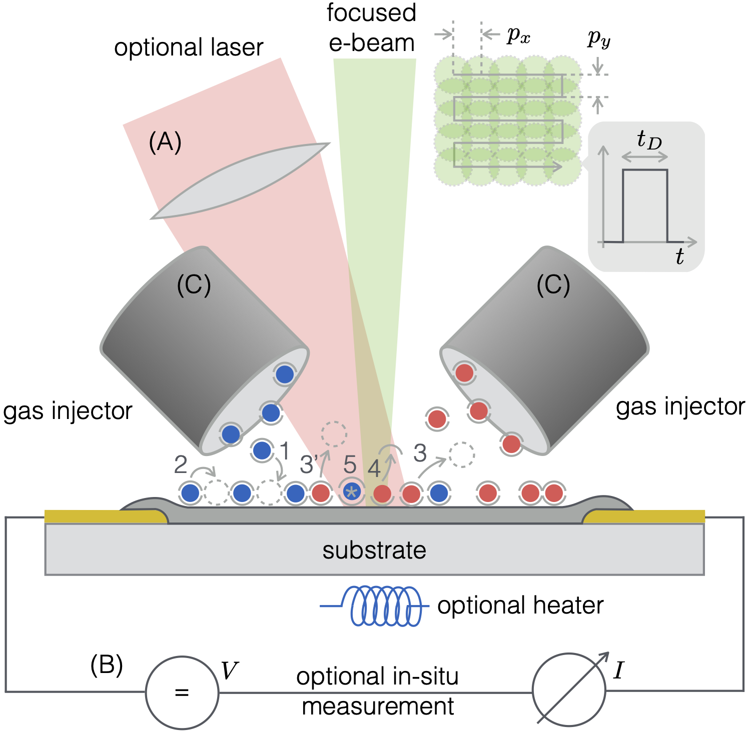
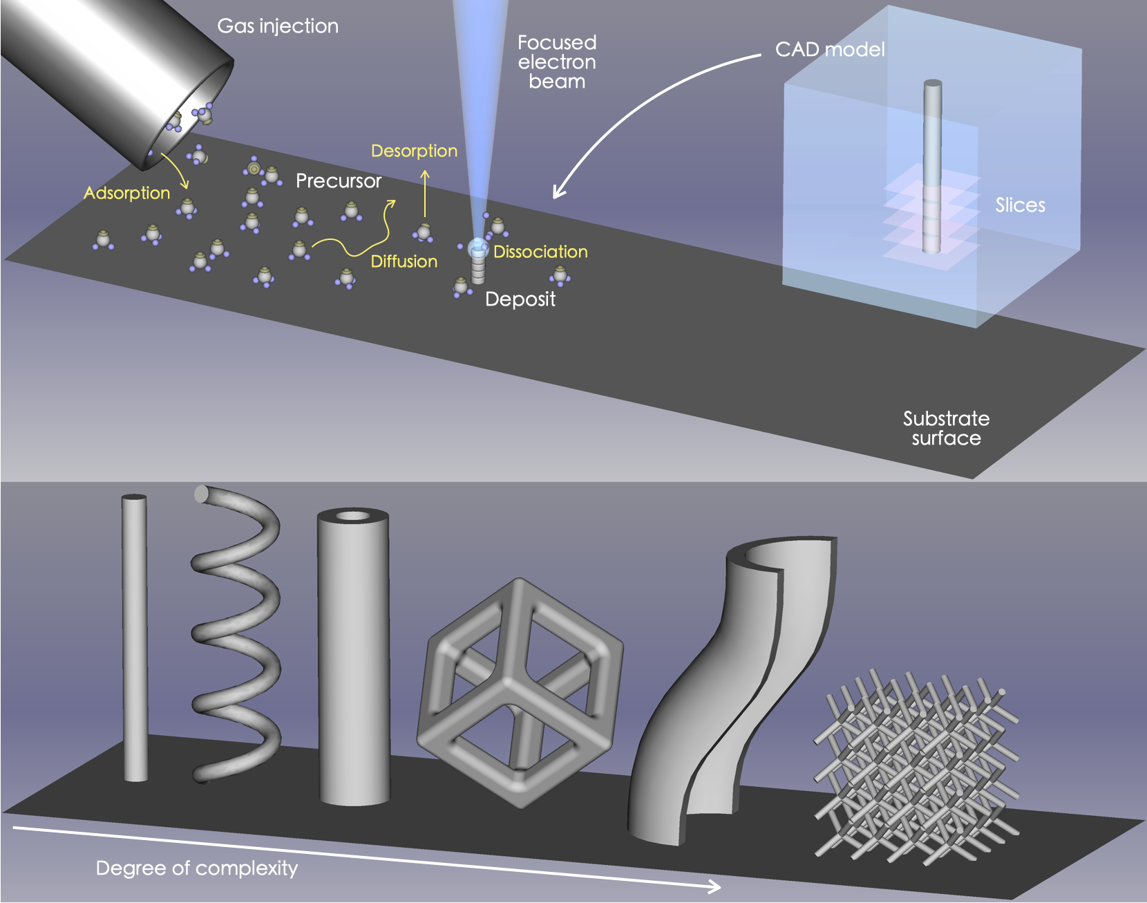
Focused Electron Beam Induced Deposition
Focused electron beam induced deposition (FEBID) is a direct-writing approach for the
fabrication of 2D- and 3D-nanostructures. Over the last decade FEBID or, more generally,
focused electron beam induced processing (FEBIP) has developed from a rather exotic
technique, employed by a small number of specialist groups for a rather limited but
important selection of applications, such as mask repair, into a highly versatile technology
for various materials research areas.
Focused electron beam induced deposition is a maskless, direct write, free form deposition
technique with an intrinsic resolution better than 10 nm. It is not limited to two dimensional (2D)
structures but is capable to 'print' three dimensional (3D) nanostructures of different materials,
like insulators, metals, magnetic materials, granular metals or superconductors on a variety of substrates.
3D nano-architectures are distinct from traditional bulk systems as they represent
low-dimensional structures expanded in a designed way into the third dimension.
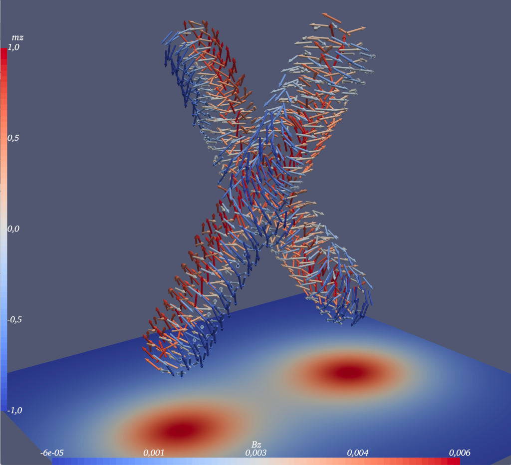
In magnetic 3D nano-objects, magnetization configurations expand not only in the plane
but also in the vertical direction, allowing one to design complex, hierarchical systems
with emerging effects which enable novel functionalities.
Granular Electronic Systems
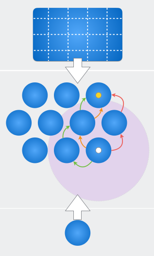
In granular electronics systems superconducting, metallic or semiconducting nanoparticles (grains)
are embedded into a non-conducting matrix or regions of increased electron density form
spontaneously in an otherwise homogeneous material.
The electronic properties of granular electronic systems are the consequence of the
non-trivial interplay of the charge transport inside the grains and the
electronic tunnel processes between the grains.
Due to the sequential charging associated with the tunneling, the electronic transport is
highly correlated.
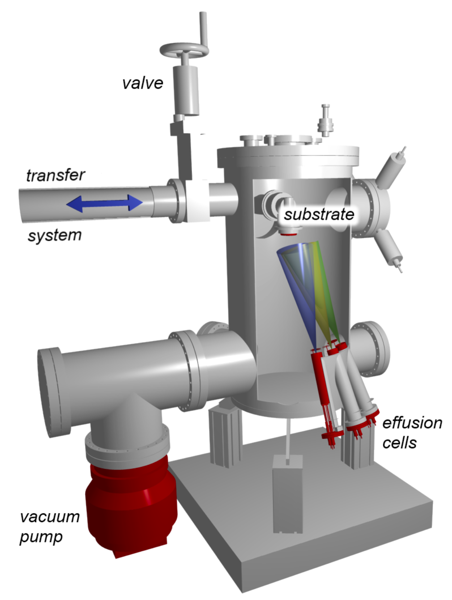
Thin film growth is pivotal for any type of device-oriented research. We employ a broad range of
thin film growth methods. These comprise Molecular Beam Epitaxy (MBE), Atomic Layer Deposition (ALD),
sputtering and simple evaporation. For microstructural, topographic and elementalanalysis we use
X-ray Diffraction (XRD), Atomic Force Microscopy (AFM), Scanning Electron Microscopy (SEM) and
Energy-Dispersive X-ray Analysis (EDX). Our focus is on epitaxial intermetallic compounds with
non-trivial magnetic ground state or strong electronic correlation effects.
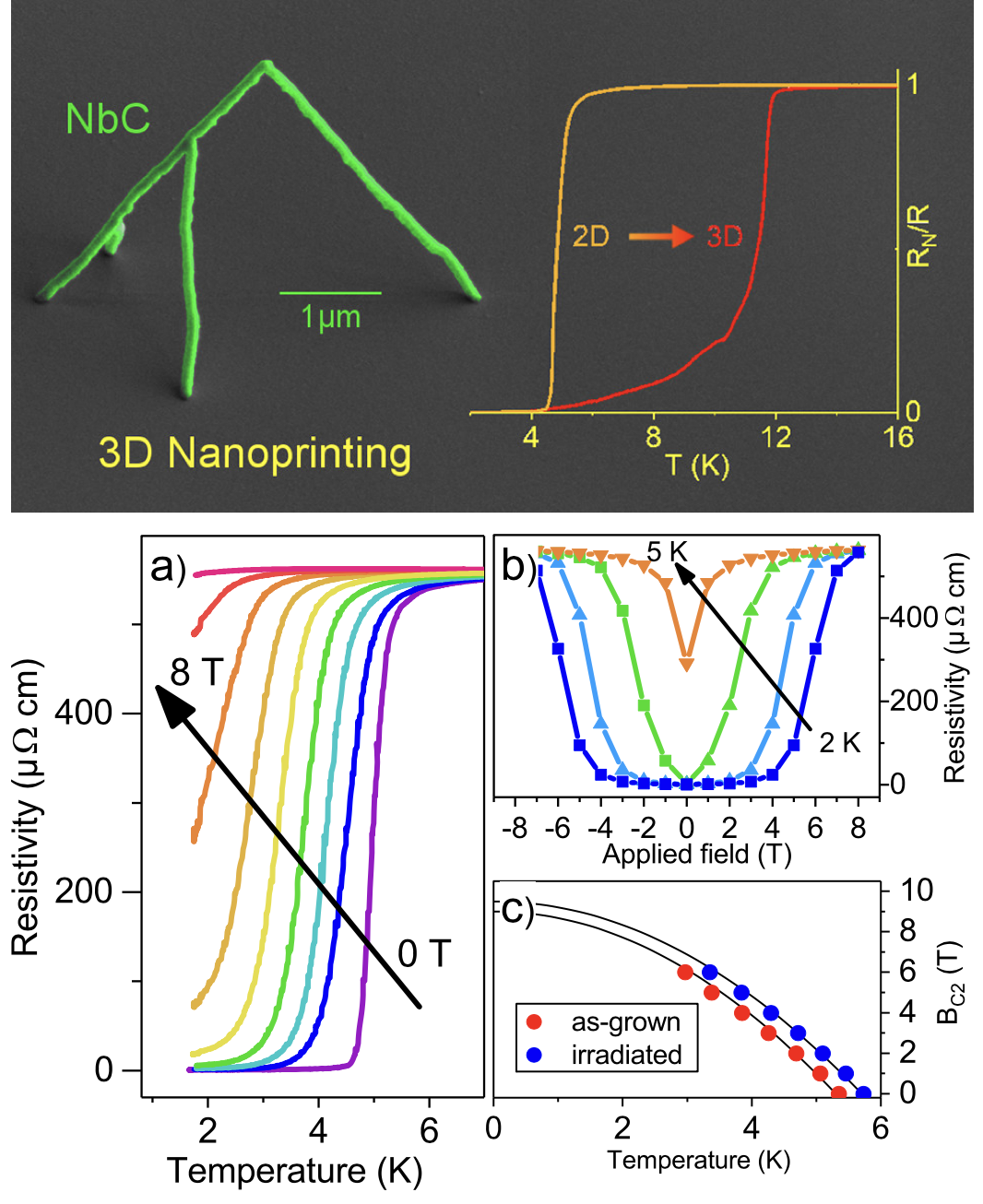
Superconductors, i.e. materials which allow dissipation-less charge transport, are one of the
most fascinating materials class in condended matter physics. We focus on both, the fabrication of
epitaxial thin films of superconductors and develop new direct-write
approaches for superconducting nanostructures by focused electron/ion beam induced deposition
(FEBID/FIBID). With thin films we mostly address the various dynamical
states of Abrikosov vortices. With our direct-write superconductors research is predominantly directed
towards the interplay of Josephson coupling and charging in nanostructures.